5A22 CPU pinout
Moderator: ZSNES Mods
5A22 CPU pinout
Does any of the dev's have the pinout of the 5A22 used in the snes? I'd be very grateful if someone could give it to me.
My general dev blog:
http://mog123x.blogspot.com
http://mog123x.blogspot.com
You could possibly, remove the 5A22, the cart connector and all the other componants on a snes mother board, and using your multimeter and all the patience you can muster, could deduce most of the pin functions of the chip.
You could certainly, track down all the address lines of Bus A, dunno about Bus B though. you could also track down the data lines aswell (using this method).
All this is assuming you know the cart connector pinnout in advance
You could certainly, track down all the address lines of Bus A, dunno about Bus B though. you could also track down the data lines aswell (using this method).
All this is assuming you know the cart connector pinnout in advance
Hardware means nothing if you don't have good software.
Compare the success of SNES over Genisis
Compare the success of SNES over Genisis
-
grinvader
- ZSNES Shake Shake Prinny
- Posts: 5632
- Joined: Wed Jul 28, 2004 4:15 pm
- Location: PAL50, dood !
Since the 5a22 is based on the 65c816, I think the pinouts are similar.
So...
So...
Code: Select all
           /=============\                     /=============\
       VP  I1          40I RES            Vss  I1          40I RES
      RDY  I2          39I VDA            RDY  I2          39I o2 (OUT)
    ABORT  I3          38I M/X       o1 (OUT)  I3          38I SO
      IRQ  I4          37I o2 (IN)        IRQ  I4          37I o2 (IN)
       ML  I5          36I BE              NC  I5          36I NC
      NMI  I6          35I E              NMI  I6          35I NC
      VPA  I7          34I R/W           SYNC  I7          34I R/W
      VDD  I8          33I D0/BA0         Vdd  I8          33I D0
       A0  I9  W65C816 32I D1/BA1          A0  I9   6502   32I D1
       A1  I10         31I D2/BA2          A1  I10         31I D2
       A2  I11         30I D3/BA3          A2  I11         30I D3
       A3  I12         29I D4/BA4          A3  I12         29I D4
       A4  I13         28I D5/BA5          A4  I13         28I D5
       A5  I14         27I D6/BA6          A5  I14         27I D6
       A6  I15         26I D7/BA7          A6  I15         26I D7
       A7  I16         25I A15             A7  I16         25I A15
       A8  I17         24I A14             A8  I17         24I A14
       A9  I18         23I A13             A9  I18         23I A13
      A10  I19         22I A12            A10  I19         22I A12
      A11  I20         21I Vss            A11  I20         21I Vss
           \=============/                     \=============/

Notes:
   ML: Memory Lock line (pin 5) is asserted low during the execution of
       the read-modify-write (asl,dec,inc,lsr,rol,ror,trb, and tsb
       instructions to inform other ics that the bus may not be claimed
       yet.

   VP: Vector Pull is asserted whenever any of the hardware vector
       address's are being accessed during an IRQ.

 Abort:  An input.  When asserted caused the current instruction to be
         aborted.

   VPA/VDA.  Valid Program Address and Valid Data Address.  These two
             signals extend on the 6502 SYNC line - to better handle
             DMA schemes.

       VPA   VDA
        0     0  -Internal Operation
        0     1  -Valid program address
        1     0  -Valid data address
        1     1  -Opcode fetch

    M/X: Memory and Index lines.  These signals are multiplexed on pin
         38.  M is available during phase zero and X during Phase one.
         These two signals reflect the contents of the status register
         m and x flags, allowing other devices to decode opcode fetches.

    E: Emulation pin.  This signal reflects the state of the processors
       emulation bit (E).

TOC

  ------------------------------------------------------------------------

===================================================================
44 PIN PLCC Pinout.

                    A
                    B
                    O               R           0
            M   I   R   R   V   V   E   V   M   2
            L   R   T   D   P   S   S   D   /   I   B
            B   Q   B   Y   B   S   B   A   X   N   E
           /----I---I---I---I---I---I---I---I---I---I-\
          / 6   5   4   3   2   1  44  43  42  41  40 I
    NMIB I 7                                       39 - E
     VPA I 8                                       38 - R/WB
     VDD I 9                                       37 - VDD
      A0 I 10                                      36 - D0/BA0
      A1 I 11                                      35 - D1/BA1
     VSS I 12               W65C816S               34 - D2/BA2
      A2 I 13                                      33 - D3/BA3
      A3 I 14                                      32 - D4/BA4
      A4 I 15                                      31 - D5/BA5
      A5 I 16                                      30 - D6/BA6
      A6 I 17                                      29 - D7/BA7
         I 18  19  20  21  22  23  24  25  26  27  28 I
         \--l---l---l---l---l---l---l---l---l---l---l-/
            A   A   A   A   A   V   V   A   A   A   A
            7   8   9   1   1   S   S   1   1   1   1
                        0   1   S   S   2   3   4   5

                   44 pin W65C816S PLCC Pinout


TOC

           -----------------------------------------------------
皆黙って俺について来い!!
Pantheon: Gideon Zhi | CaitSith2 | Nach | kode54
Code: Select all
<jmr> bsnes has the most accurate wiki page but it takes forever to load (or something)The 5A22 is a 100 pin IC package
Also, the 40 pin DIP "65C816" you have shown, grinvader, is actualy a 65C802, which is a CPU that is a pin and instruction compadible upgrade for the 6502.
It lacks the address lines from A16 through to A23 (which th 65816 has)and it also lacks the extra 8-bit address bus (Bus B), specific to the 5A22.
Last edited by declan on Tue Mar 25, 2008 9:11 am, edited 1 time in total.
Hardware means nothing if you don't have good software.
Compare the success of SNES over Genisis
Compare the success of SNES over Genisis
You could also find the pins for the controller ports, like Clock 1 & 2, Latch 1 & 2, Data 1 & 2.declan wrote:You could certainly, track down all the address lines of Bus A, dunno about Bus B though. you could also track down the data lines aswell (using this method).
There you go, another 6 pins of 100, solved!
Hardware means nothing if you don't have good software.
Compare the success of SNES over Genisis
Compare the success of SNES over Genisis
Oh sh****....sugar
How could i have forgoten.
CaitSith2 has a Zip file on his/her (i'm not sure which) website, containing snes schematics.
This sould have the 5A22 and its pinout.
Here's the link to the main page
Click on "SNES Schematics".
How could i have forgoten.
CaitSith2 has a Zip file on his/her (i'm not sure which) website, containing snes schematics.
This sould have the 5A22 and its pinout.
Here's the link to the main page
Click on "SNES Schematics".
Hardware means nothing if you don't have good software.
Compare the success of SNES over Genisis
Compare the success of SNES over Genisis
The schematics reveal some interesting facts, which could be used to find out how the SNES works in detail.
Bot PPU's are communicating via an 18bit data bus with each other. Quite unusual is the fact that PPU1 has 2 address buses going to each 32k SRAM, they probably did this so that in Mode 7, you could fetch 2 8bit pixels from seperate locations . It also seems that PPU1 does all the adressing, while PPU2 can only access the data from the SRAMS. My guess is that PPU2 holds all the colour registers and at least 2 line buffers for the main and sub screen and does all colour calculations. They most probably used line buffers, because it faciliates the following features:
- main / sub screen colour arithmetic
- mosaic effect (just update every nth pixel / line in the buffer).
- sprite display (a line buffer for everything is less complex than having 34 shift registers for each sprite, you just need 1 shift register and write sprite data into the line buffer at the right x address)
Both PPU's and the CPU have access to the 21Mhz master clock, but PPU2 also has 2 seperate signals (X & Y) going to the CPU, which is probably switching the CPU speed (4 states could be decoded).
I think this is worth an own topic...
-
creaothceann
- Seen it all
- Posts: 2302
- Joined: Mon Jan 03, 2005 5:04 pm
- Location: Germany
- Contact:
Just to be sure: 2 address buses per 32K chip, or 1 address bus per chip?Vigo wrote:Quite unusual is the fact that PPU1 has 2 address buses going to each 32k SRAM, they probably did this so that in Mode 7, you could fetch 2 8bit pixels from seperate locations .
I'd guess it's the HIRQ/VIRQ lines.Vigo wrote:Both PPU's and the CPU have access to the 21Mhz master clock, but PPU2 also has 2 seperate signals (X & Y) going to the CPU, which is probably switching the CPU speed (4 states could be decoded).
This seems to be currently unused though.Vigo wrote:I think this is worth an own topic...
vSNES | Delphi 10 BPLs
bsnes launcher with recent files list
bsnes launcher with recent files list
There are 2 * 32k SRAM chips, and each chip is connected to the PPU through its own data AND address bus. Normally, you would have only one address bus for both chips, which would work for all character modes, except mode 7, where the hardware needs to be more flexible in reading pixel data from different locations each.creaothceann wrote:Just to be sure: 2 address buses per 32K chip, or 1 address bus per chip?Vigo wrote:Quite unusual is the fact that PPU1 has 2 address buses going to each 32k SRAM, they probably did this so that in Mode 7, you could fetch 2 8bit pixels from seperate locations .
Hmm, I suppose you could be right, but then I'd suggest its the IRQ and NMI lines.I'd guess it's the HIRQ/VIRQ lines.Vigo wrote:Both PPU's and the CPU have access to the 21Mhz master clock, but PPU2 also has 2 seperate signals (X & Y) going to the CPU, which is probably switching the CPU speed (4 states could be decoded).
-
byuu
It's for interleaving data. Can help with multiple things, including mode 7. Hard to say, we know next to nothing about low-level PPU operation.Quite unusual is the fact that PPU1 has 2 address buses going to each 32k SRAM
It renders in real-time, there's no full line buffer involved. You can change color (note the lack of a u in color, Britain) registers mid-scanline and see the changes. One thing it does seem to do is buffer sprite stuff on the previous scanline.My guess is that PPU2 holds all the colour registers and at least 2 line buffers for the main and sub screen and does all colour calculations.
If you really care, you should probably read up on NES PPU emulation, which is light years ahead of us. The SNES is similar in many ways, just a whole lot more complex.
No, it would be horizontal and vertical retrace signals. The PPU doesn't know anything about when to trigger IRQs. It could BS NMIs, of course, but that's not what it does. That's the CPU's job.Hmm, I suppose you could be right, but then I'd suggest its the IRQ and NMI lines.
The CPU has its own counters that go off the PPU h/vblank states. CPU is aware of its own cycle counts and adds them normally. When PPU H goes low, it increments the V counter. When PPU V goes low, it resets the V counter. The are out of alignment by two clock cycles against the 21MHz clock, and this causes / explains some interesting edge cases with IRQs as you would expect.
You don't need 2 address buses for interleaving data. It most probably fetches 2 bitplanes from each character in one word cycle. Since those 2 bitplanes are on the same word address, both address buses will have the same value at this point. The only application I can really think of where 2 address buses, 2 different addresses for each byte, are needed is mode 7, where 2 neighboring 8bit pixels could be coming from different characters.byuu wrote:It's for interleaving data. Can help with multiple things, including mode 7. Hard to say, we know next to nothing about low-level PPU operation.Quite unusual is the fact that PPU1 has 2 address buses going to each 32k SRAM
Actually, it's Germany, but thanks.It renders in real-time, there's no full line buffer involved. You can change color (note the lack of a u in color, Britain)My guess is that PPU2 holds all the colour registers and at least 2 line buffers for the main and sub screen and does all colour calculations.
Of course, but that doesn't explain if there is a line buffer or not. With line buffer, I mean that in 1 buffer, one line is being rendered while the other is being displayed and vice versa. That would essentially mean that the video output is always 1 line behind. The other possibility is that the line buffer is being updated the same time it is being read.registers mid-scanline and see the changes.
The thing which brings me to this idea is that it would be the easiest way to implement the sprites and the mosaic effect. The SNES most certainly does not have 32 4bit deep shift registers, the priotity and X detection logic alone would be immense and consume much chip space. Rendering to a 256 pixel line buffer however is much more straightforward. Priority is achieved in what order sprite pixels are written into the buffer (high priority sprites are overwriting sprite pixel data of previously rendered low priority sprites), and the X position is just the starting address of the line buffer byte. Many arcade games do it this way.
To acconplish the Mosaic effect, you would just have to suspend rendering INTO the line buffer for each repeated Y pixel expansion, which is much more easier than having the character/sprite fetch address logic generating the appropriate addresses to accomplish this effect: it would have to hold addresses for the y-repetition of pixels, and then add values for the next pixel block to those adresses to compensate for skipped y pixels -> too complicated in hardware, and this is excluding mode 7... Especially considering since the pixel block can have sizes of "non power of two".
I think the mosaic effect belongs to those effects which hardware engineers add as an afterthought, because the architecture easily allows it.
Yes, the sprite engine is being started 1 line earlier to evaluate what sprites are in range, since sprite data fetches most certainly occur in HBLANK, which means that the evaluation has to be finished before the first display line starts.One thing it does seem to do is buffer sprite stuff on the previous scanline.
I know the NES PPU document, but, as you put it, the SNES is more complex. There are similarities (the whole pixel video timing for example, and the way the sprite evaluation works. Interestingly, both aspects have been copied from the TMS9918 working in the Colecovision) and there are things which are obviously more advanced. The NES has only 8 2bit wide sprites per line, for that, a whole line buffer is a waste of logic gates.If you really care, you should probably read up on NES PPU emulation, which is light years ahead of us. The SNES is similar in many ways, just a whole lot more complex.
Ah, ok, you are right, I see now that the H/V registers are in CPU register space ($4xxx). It's strange that Nintendo implemented the H/V counters in the CPU, effectively replicating what is already contained in the PPUs.No, it would be horizontal and vertical retrace signals. The PPU doesn't know anything about when to trigger IRQs. It could BS NMIs, of course, but that's not what it does. That's the CPU's job.
The CPU has its own counters that go off the PPU h/vblank states. CPU is aware of its own cycle counts and adds them normally. When PPU H goes low, it increments the V counter. When PPU V goes low, it resets the V counter. The are out of alignment by two clock cycles against the 21MHz clock, and this causes / explains some interesting edge cases with IRQs as you would expect.
Better late than never
Might as well just give this away now.
Edit: New document from no$ explains pins 83 and 84. These are the X and M flags of the Status Register. (I hope).
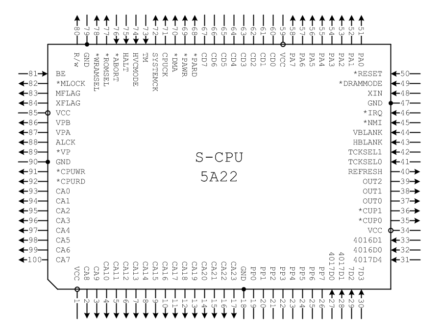
In the SNES:
4017D2, 4017D3, 4017D4, *DRAMMODE, TCKSEL0, TCKSEL1, TM, HVCMODE, and HALT are all tied low.
*NMI, *ABORT, and PE are tied high. I would assume PE is something like peripheral enable, it's not the E-Clock output. EDIT: Pin 81 renamed to BE (Bus Enable). Active high.
OUT[2..1], PP[5..0] (parallel port), *DMA, CPUCK, R/w, *VP, VPA, VPB, "MFLAG", "XFLAG", and *MLOCK don't connect anywhere.
The PA_ stuff is known otherwise as the B-Bus.
CA_ and CD_ are the normal CPU address and data busses. I put a C in front, because when I do schematic layout with the roms and RAM chips, there's that whole issue with A15 being used or not in LoRom / HiRom configurations. The RAM and ROM chips just have A0..A19 or whatever.
Edit: New document from no$ explains pins 83 and 84. These are the X and M flags of the Status Register. (I hope).
In the SNES:
4017D2, 4017D3, 4017D4, *DRAMMODE, TCKSEL0, TCKSEL1, TM, HVCMODE, and HALT are all tied low.
*NMI, *ABORT, and PE are tied high. I would assume PE is something like peripheral enable, it's not the E-Clock output. EDIT: Pin 81 renamed to BE (Bus Enable). Active high.
OUT[2..1], PP[5..0] (parallel port), *DMA, CPUCK, R/w, *VP, VPA, VPB, "MFLAG", "XFLAG", and *MLOCK don't connect anywhere.
The PA_ stuff is known otherwise as the B-Bus.
CA_ and CD_ are the normal CPU address and data busses. I put a C in front, because when I do schematic layout with the roms and RAM chips, there's that whole issue with A15 being used or not in LoRom / HiRom configurations. The RAM and ROM chips just have A0..A19 or whatever.
Last edited by whicker on Mon Feb 27, 2012 3:59 am, edited 2 times in total.
-
Grigori
Re: 5A22 CPU pinout
Well ultimately it's for mode 7 and for interleaved data. Because in mode 7, the name table and tile data are interleaved, with the name table stored in the low byte and tile data in the high byte of every word.Vigo wrote:You don't need 2 address buses for interleaving data. It most probably fetches 2 bitplanes from each character in one word cycle. Since those 2 bitplanes are on the same word address, both address buses will have the same value at this point. The only application I can really think of where 2 address buses, 2 different addresses for each byte, are needed is mode 7, where 2 neighboring 8bit pixels could be coming from different characters.
They have to be stored interleaved, because the VRAM is clocked at 5.37 MHz, which is also the pixel clock. Because mode 7 allows for free scaling and rotation of the background, there's no guarantee that pixels that are adjacent on screen are contiguous in VRAM - thus it needs to load name table data and tile data every pixel, rather than every tile. But because the PPU can only read 1 word of VRAM every pixel, the name table and tile data need to be interleaved, and the PPU needs to be able to read the high and low bytes from different words - thus there are two separate VRAM address buses, one for the low byte, and one for the high byte.
So every pixel clock, the PPU reads the name table data for the next pixel from the low byte while reading the current pixel's color data from the high byte.
This is also why mode 7 tiles are stored in packed-pixel format, instead of the planar format of all other tile data.
The PPU has a single linebuffer, but it is used for sprites only. (The linebuffer is actually composed of 2 128x9-bit linebuffers, each one storing 4 bits of color data, 3 bits for palette number, and 2 priority bits - one linebuffer stores the even-numbered pixels,the other stores the odd-numbered pixels. The linebuffers are clocked at 10.7 MHz when being written to, and have separate address lines; this arrangement means that 4 pixels can be written to the linebuffer every pixel clock.) It only needs 1 linebuffer, because memory access patterns dictate that it's impossible to render sprites while they're being displayed.Of course, but that doesn't explain if there is a line buffer or not. With line buffer, I mean that in 1 buffer, one line is being rendered while the other is being displayed and vice versa. That would essentially mean that the video output is always 1 line behind. The other possibility is that the line buffer is being updated the same time it is being read.
The thing which brings me to this idea is that it would be the easiest way to implement the sprites and the mosaic effect. The SNES most certainly does not have 32 4bit deep shift registers, the priotity and X detection logic alone would be immense and consume much chip space. Rendering to a 256 pixel line buffer however is much more straightforward. Priority is achieved in what order sprite pixels are written into the buffer (high priority sprites are overwriting sprite pixel data of previously rendered low priority sprites), and the X position is just the starting address of the line buffer byte. Many arcade games do it this way.
To acconplish the Mosaic effect, you would just have to suspend rendering INTO the line buffer for each repeated Y pixel expansion, which is much more easier than having the character/sprite fetch address logic generating the appropriate addresses to accomplish this effect: it would have to hold addresses for the y-repetition of pixels, and then add values for the next pixel block to those adresses to compensate for skipped y pixels -> too complicated in hardware, and this is excluding mode 7... Especially considering since the pixel block can have sizes of "non power of two".
I think the mosaic effect belongs to those effects which hardware engineers add as an afterthought, because the architecture easily allows it.
Backgrounds are generated via shift registers, just as in the NES. There are six pairs of 16-bit shift registers, coupled to six pairs of 8-bit temporary registers, labeled a, b, c, d, e, and f. There are also 4 BG attribute registers, each connected to a delay circuit that hold its previous two values, and 4 temporary BG name registers. There are also two tile offset control words, one vertical, one horizontal.
There are four types of BG reads - name table reads, tile data reads, and offset reads. On a name table read, the attribute bits (3 for palette, 1 for priority) are stored in the appropriate attribute register, and the tile index is stored in the appropriate name register. On a tile data read, the data is written to the appropriate temporary register n, with the low byte going into temporary n0 and the high byte into temporary n1. On an offset read, the data is written to one of the tile offset control words (in mode 4, bit 15 selects which control word to write to; in other modes, bit 15 is ignored); because offset reads come after attribute data reads, the first tile on each scanline is not affected by tile offset, and the offset read affects the next set of tiles.
Finally, of course, there are mode 7 data reads, which read 8-bit color data over the high bus and the tile name for the next pixel over the low bus, and increments the mode 7 horizontal accumulators. Theses are the only transfers that will put different addresses on the two VRAM address buses. Furthermore, mode 7 completely overrides the shift registers - instead, the color data byte is used directly as the BG1 color data, and in EXTBG mode, bits 3-0 are used as BG2 color data and bits 7-4 as BG2 attribute data.
The video mode selects which shift registers are used to generate each BG's color data, and determines the PPU's read sequence (the pattern of 8 VRAM reads the PPU performs for every rendered tile).
In 1 scanline, the PPU performs 33 BG read sequences (264 pixel clocks), waits 9 pixel clocks for the active scan period to end (because video output doesn't start until 17 pixel clocks after BG reading begins), and then loads 34 sprite tiles (68 pixel clocks).
The color data from each background layer is then combined with the current pixel from the sprite linebuffer (note that the linebuffer is erased as it is read) and fed into the priority circuit to determine what is actually drawn. The PPU's internal clock rate is actually 10.7 MHz (or half the master clock), meaning each pixel takes 2 PPU clocks. The first PPU cycle of each pixel generates the sub screen pixel, and the second cycle generates the main screen pixel. The output of the color math circuit is latched every PPU clock in H 512 mode, or every other PPU clock otherwise, and is then sent to the video encoder. Because the color math output is latched every PPU clock in H 512 mode, color math does not function as expected.
The mosaic system is actually composed of two sub-systems, one for horizontal, and one for vertical.
The color data from the shift registers feed into a series of latches; these latches are controlled by the horizontal-mosaic system, which causes them to latch the color data every X pixel clocks (where X=1 if mosaic is disabled for that BG layer, or the mosaic size if it's enabled).
The PPU also maintains a vertical line counter - the vertical mosaic system latches this counter every X scanlines (again, X is the mosaic size). If mosaic is enabled for a BG layer, it uses the latched counter, otherwise it uses the normal counter. This is then added to the layer's vertical scroll register or the vertical tile offset to determine which tile data row to load. This is why you don't get a pure mosaic effect if you have mosaic active while using HDMA to change the vertical scrolling registers or mode 7 scaling/rotation registers.
Re: 5A22 CPU pinout
welcome Grigori...
uh, one question: how do you know all of this?
uh, one question: how do you know all of this?
Re: 5A22 CPU pinout
I would love to see byuu comment on Grigori's post. 
-
adventure_of_link
- Locksmith of Hyrule
- Posts: 3634
- Joined: Sun Aug 08, 2004 7:49 am
- Location: 255.255.255.255
- Contact:
Re: 5A22 CPU pinout
Holy thread bump Batman.. good job, Grigori...
And to motke, good luck... byuu has basically alienated just about everyone these days (meaning the only real way to get a hold of him is on his BSNES forum).
And to motke, good luck... byuu has basically alienated just about everyone these days (meaning the only real way to get a hold of him is on his BSNES forum).
<Nach> so why don't the two of you get your own room and leave us alone with this stupidity of yours?
NSRT here.
NSRT here.
Re: Better late than never
Hi,whicker wrote: I would assume PE is something like peripheral enable, it's not the E-Clock output.
I think you made a mistake. It's "BE", not "PE".
I stumbled upon this by incident while looking at your Pinout which BTW has helped me out nicely for building a RS-232 Interface for my SNES. Thanks !SomeGeneric65816Datasheet wrote: Bus Enable (BE)
The Bus Enable input signal allows external control of the Address and Data
Buffers, as well as the R/W signal With Bus Enable high, the R/W and Address
Buffers are active. The Data/Address Buffers are active during the first half
of every cycle and the second half of a write cycle. When BE is low, these
buffers are disabled. Bus Enable is an asynchronous signal.
Re: 5A22 CPU pinout
Post and image changed above to reflect ngevan2k's finding.
I really wish there was a better scan of the official schematics. My copy is scanned at slightly too low of contrast, skewed, folded, split into 4 parts, and saved as JPG.
I really wish there was a better scan of the official schematics. My copy is scanned at slightly too low of contrast, skewed, folded, split into 4 parts, and saved as JPG.
Re: 5A22 CPU pinout
BAH I'm with stupid(that's me). And that's a long story.whicker wrote: I really wish there was a better scan of the official schematics. My copy is scanned at slightly too low of contrast, skewed, folded, split into 4 parts, and saved as JPG.